Science & Tech
-
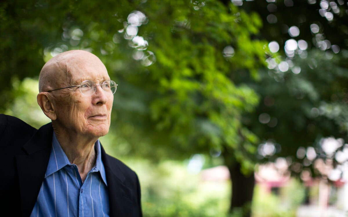
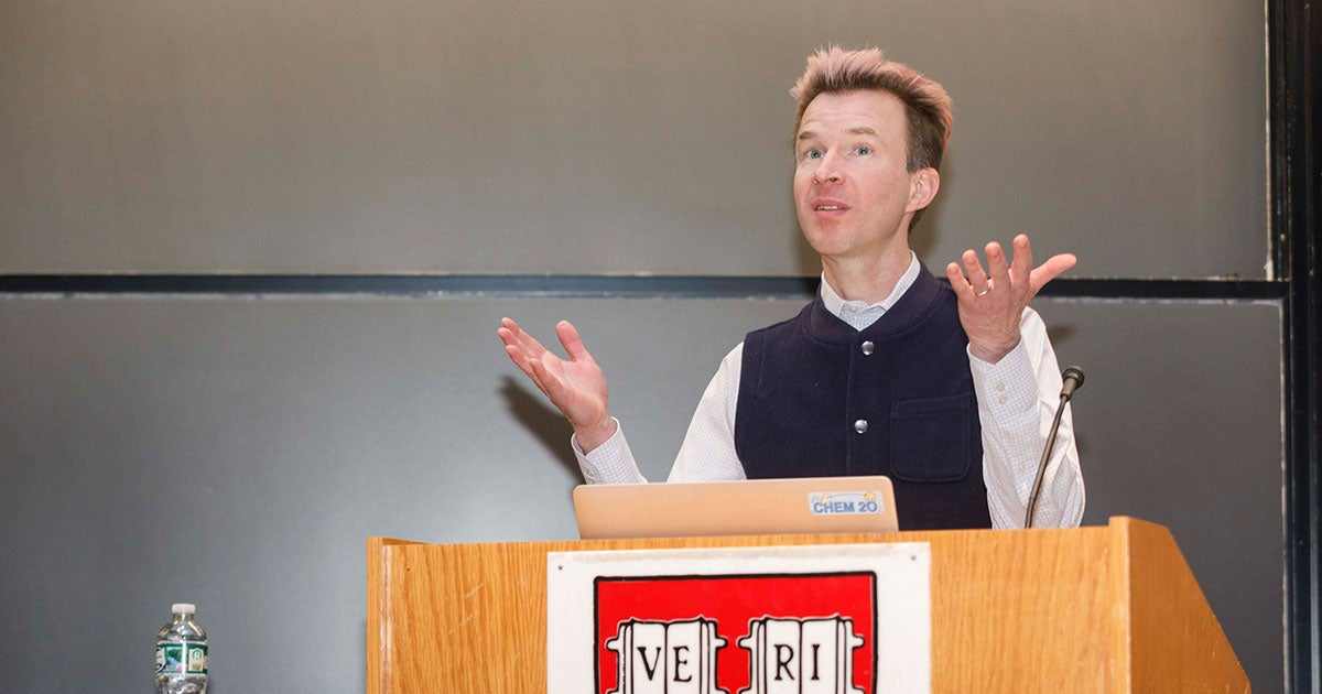
‘The scientist is not in the business of following instructions.’
George Whitesides became a giant of chemistry by keeping it simple
Part of the Experience series -
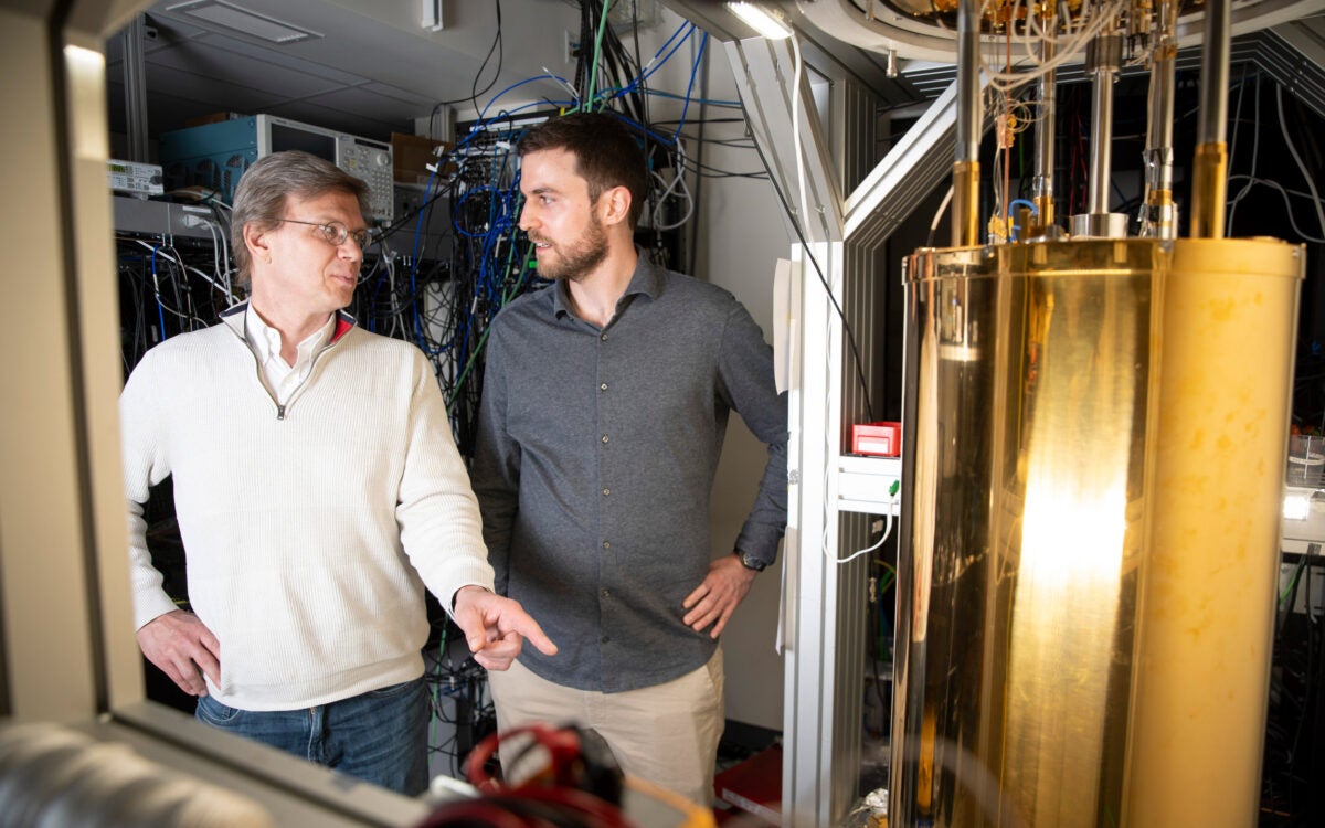
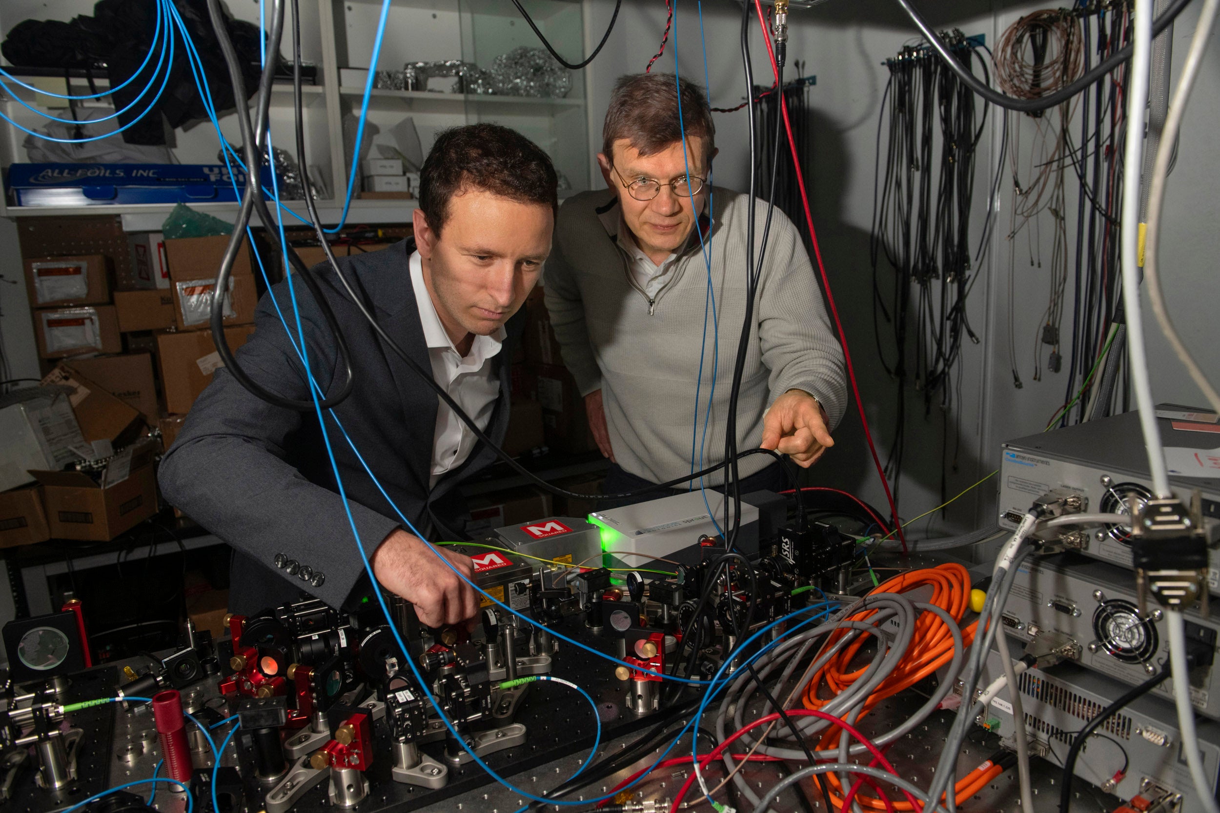
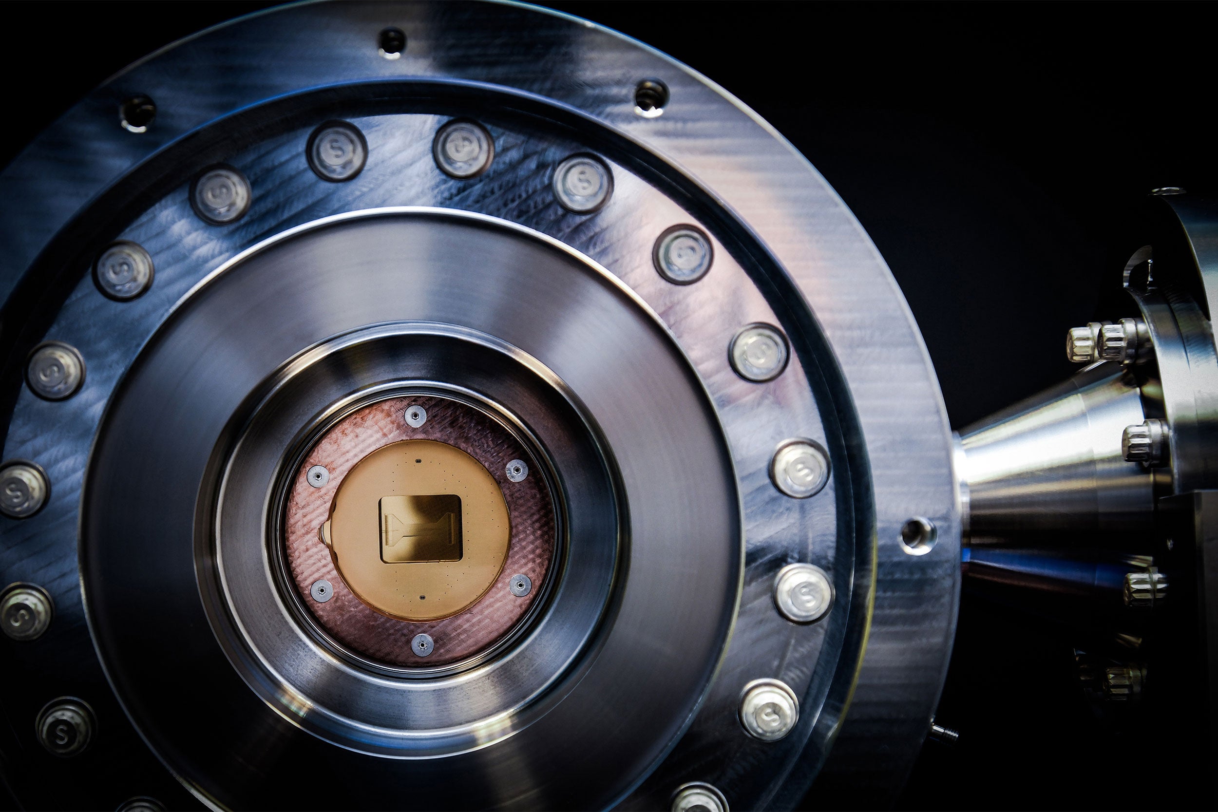
Glimpse of next-generation internet
Physicists demo first metro-area quantum computer network in Boston
Part of the Findings series -
Science is making anti-aging progress. But do we want to live forever?
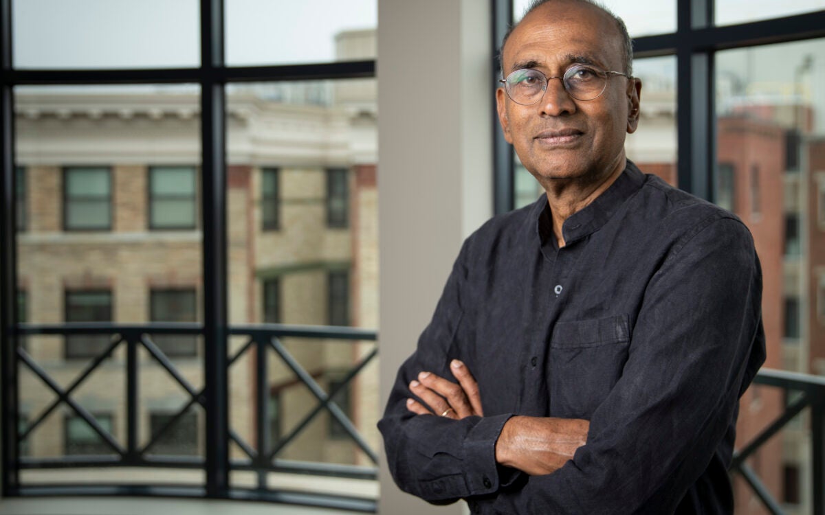
Nobel laureate details new book, which surveys research, touches on larger philosophical questions
Part of the Findings series -
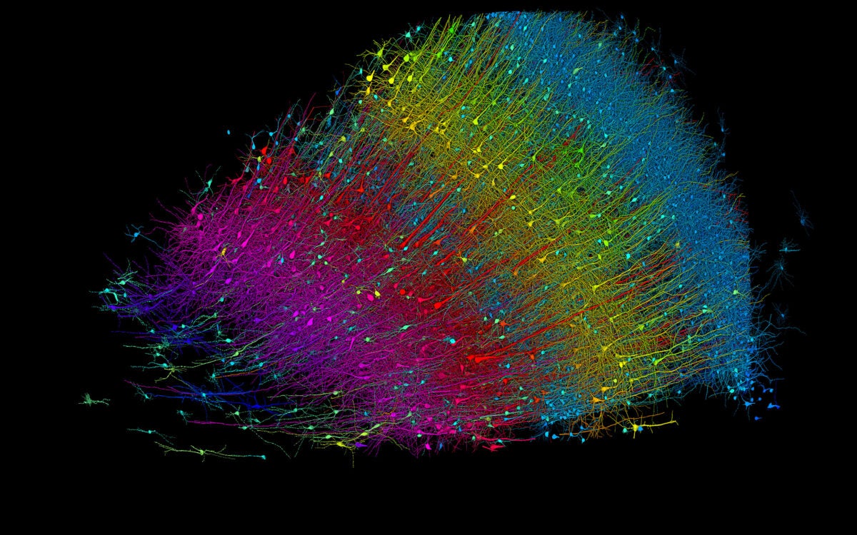
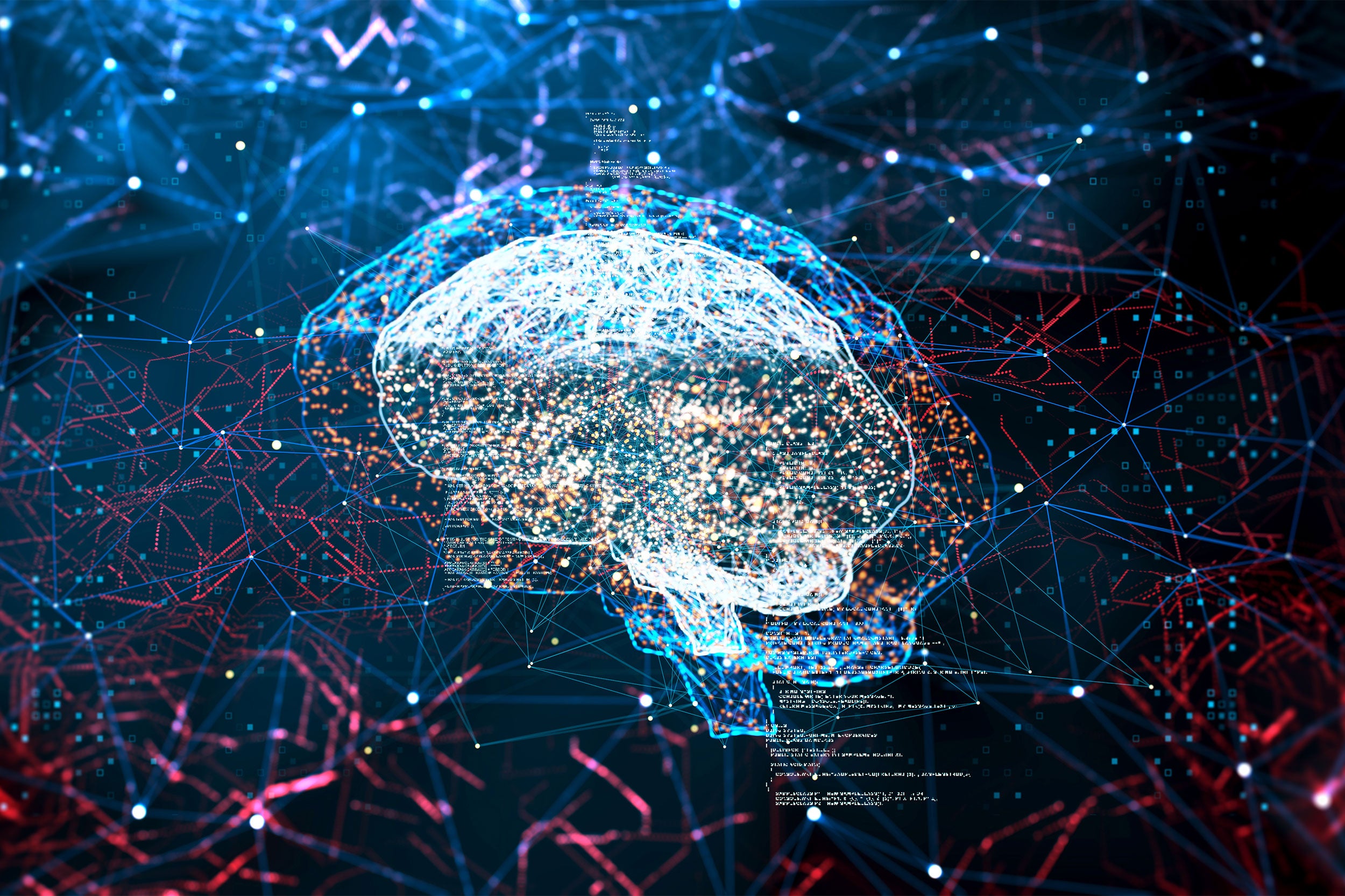
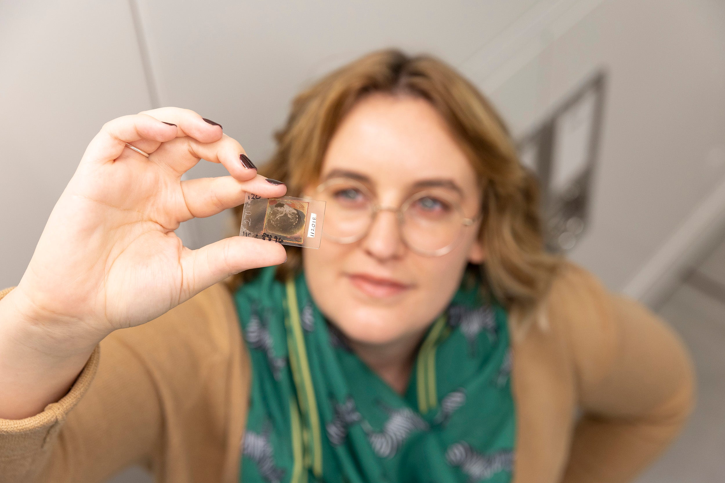
Epic science inside a cubic millimeter of brain
Researchers publish largest-ever dataset of neural connections
Part of the Findings series -
What is ‘original scholarship’ in the age of AI?
Symposium considers how technology is changing academia
-
Complex questions, innovative approaches
Seven projects awarded Star-Friedman Challenge grants
-
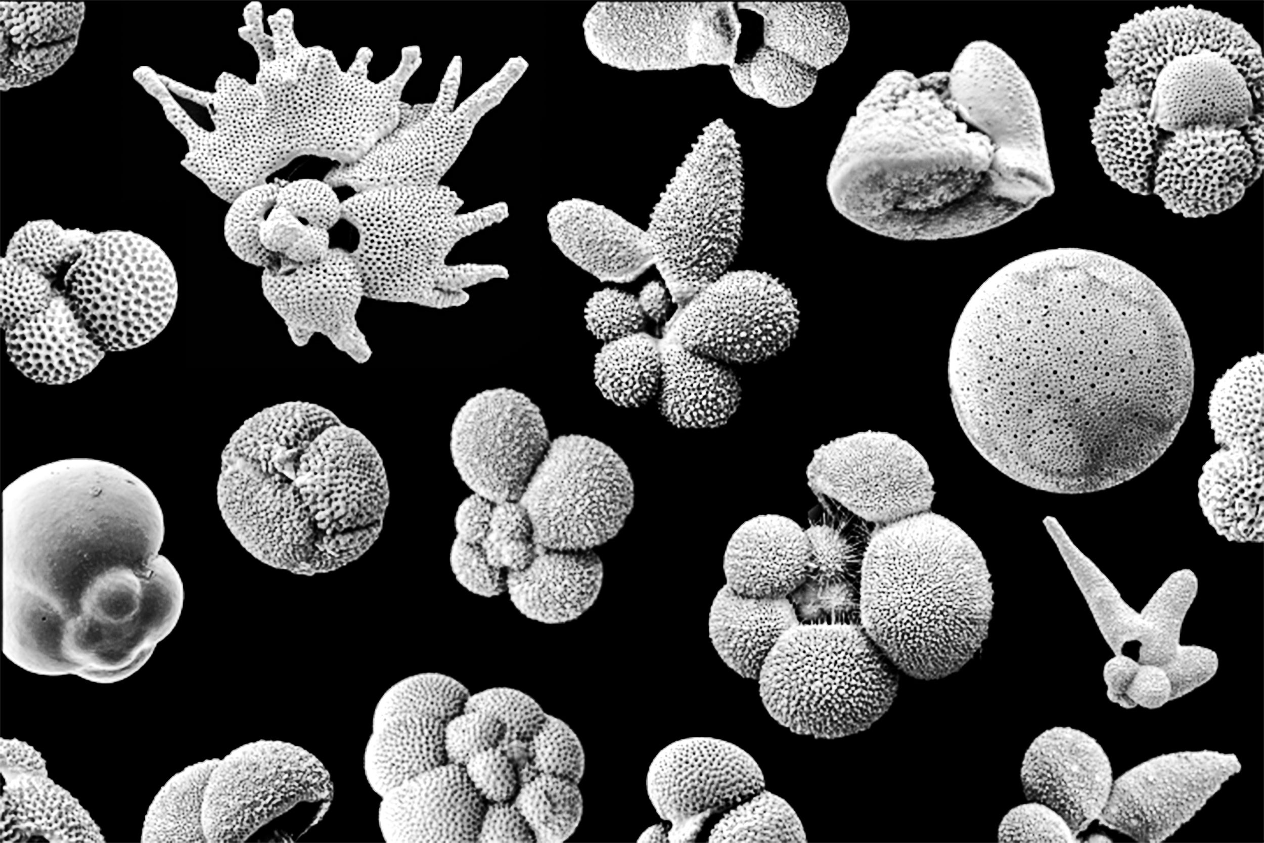
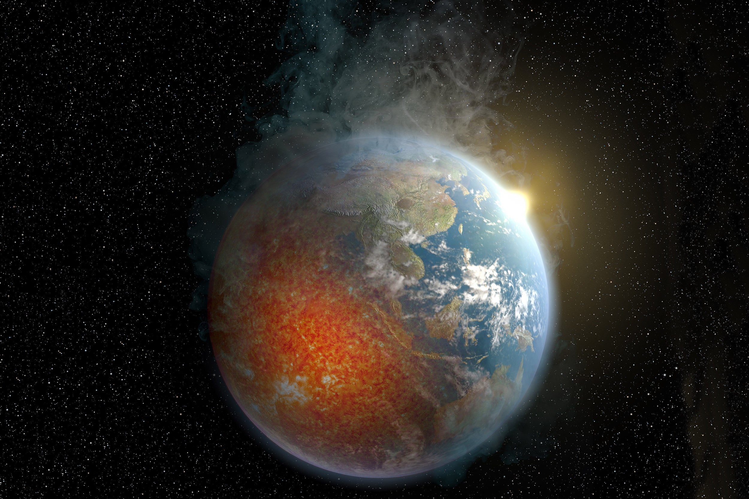
Early warning sign of extinction?
Fossil record stretching millions of years shows tiny ocean creatures on the move before Earth heats up
-
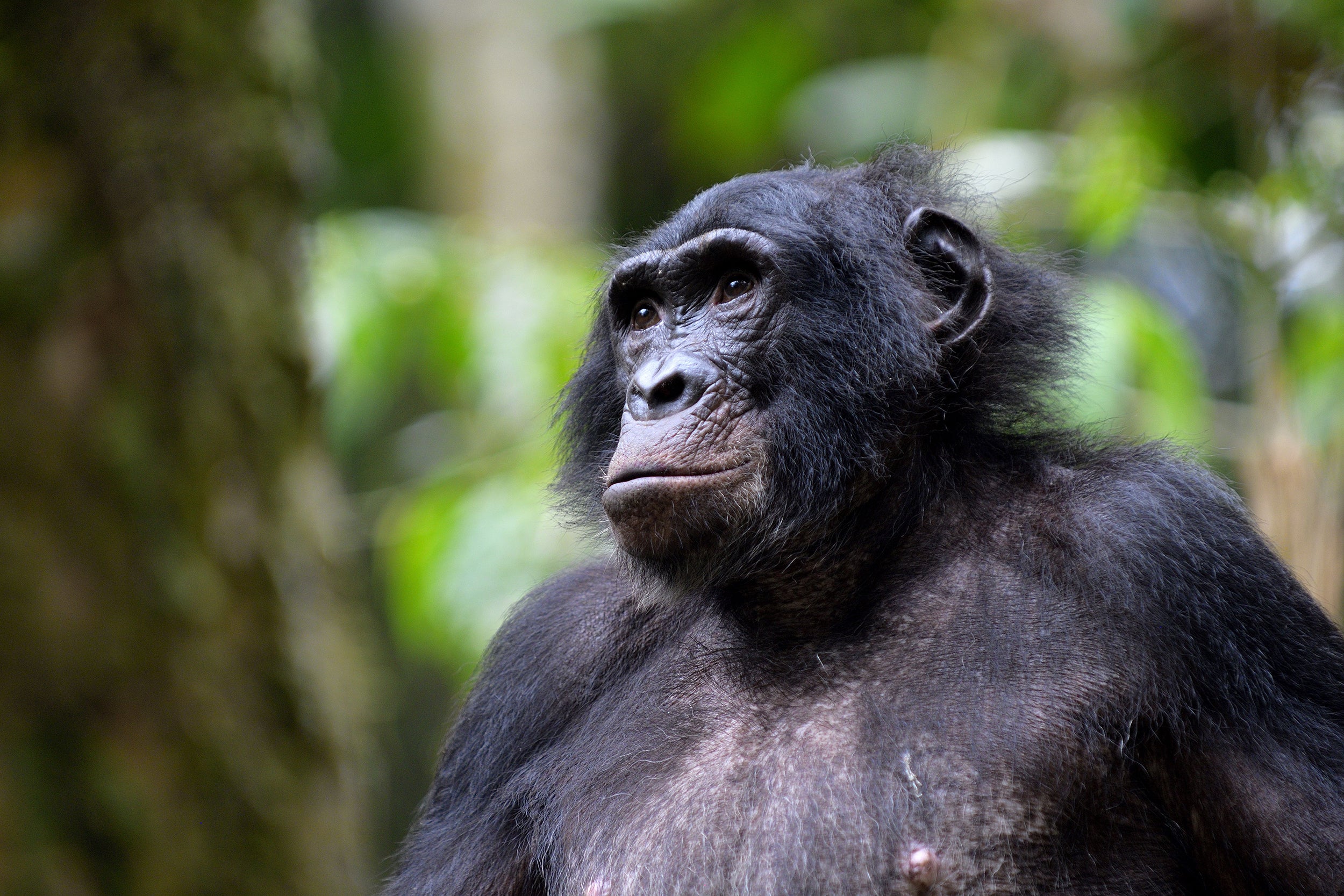
So much for summers of love
Despite ‘hippie’ reputation, male bonobos fight three times as often as chimps, study finds
-
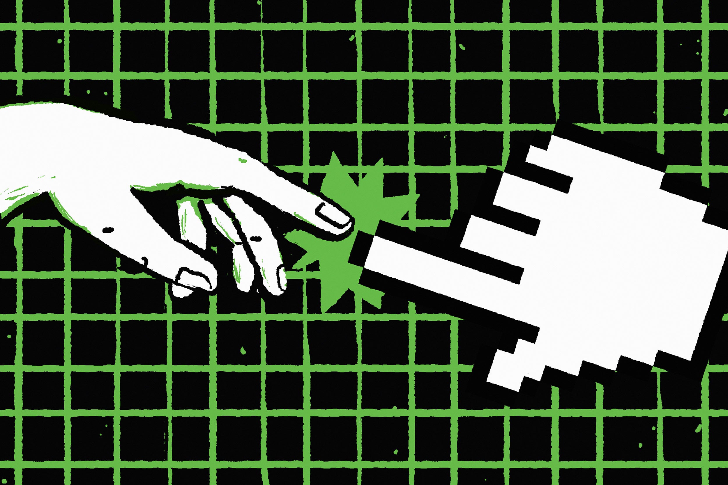
Are you a human? Select all that apply.
Philosopher Barba-Kay on CAPTCHA dilemma, Aristotle’s good life, and how the internet is changing us — not for the better
-
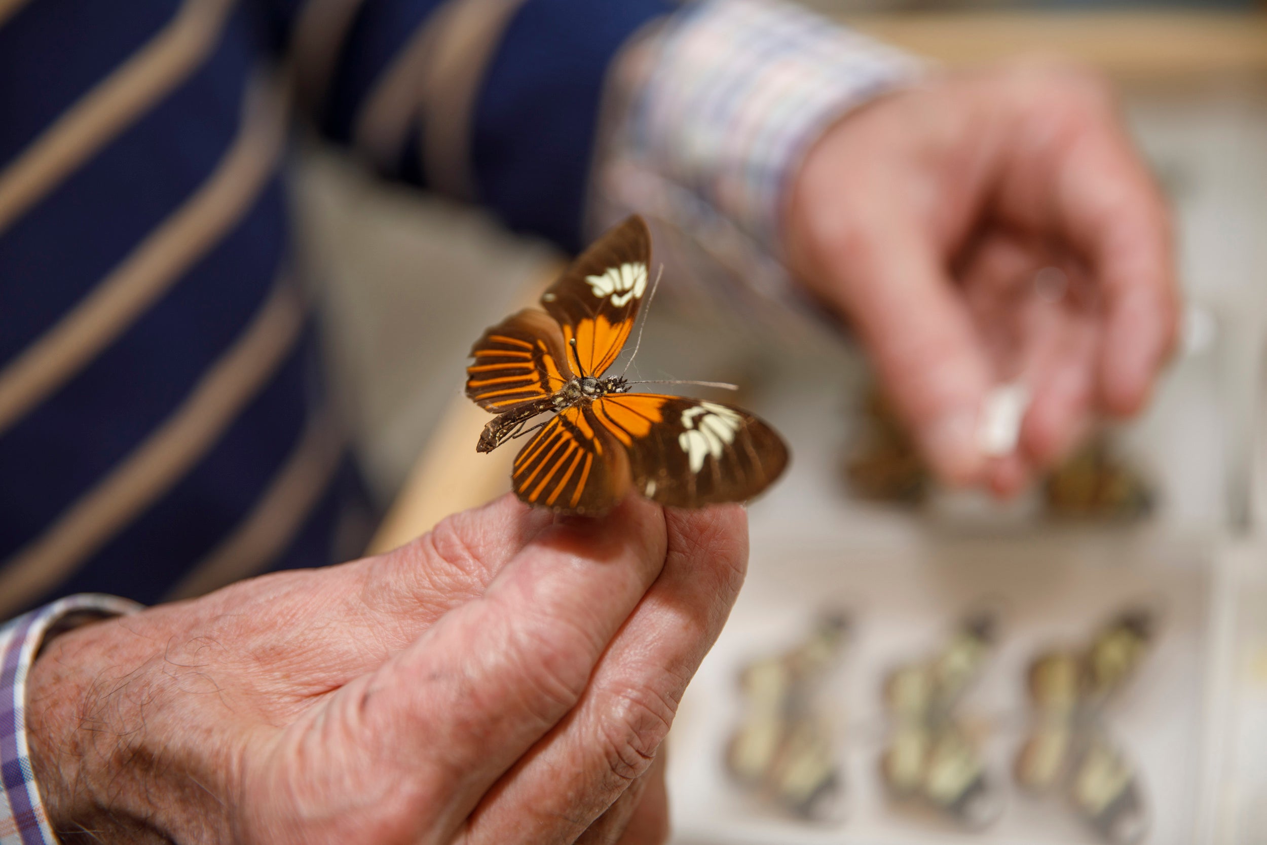
Amazon butterfly evolved from hybrids
Genomic findings challenge thinking on what makes a species
-
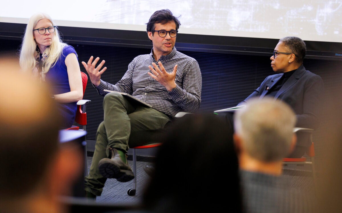
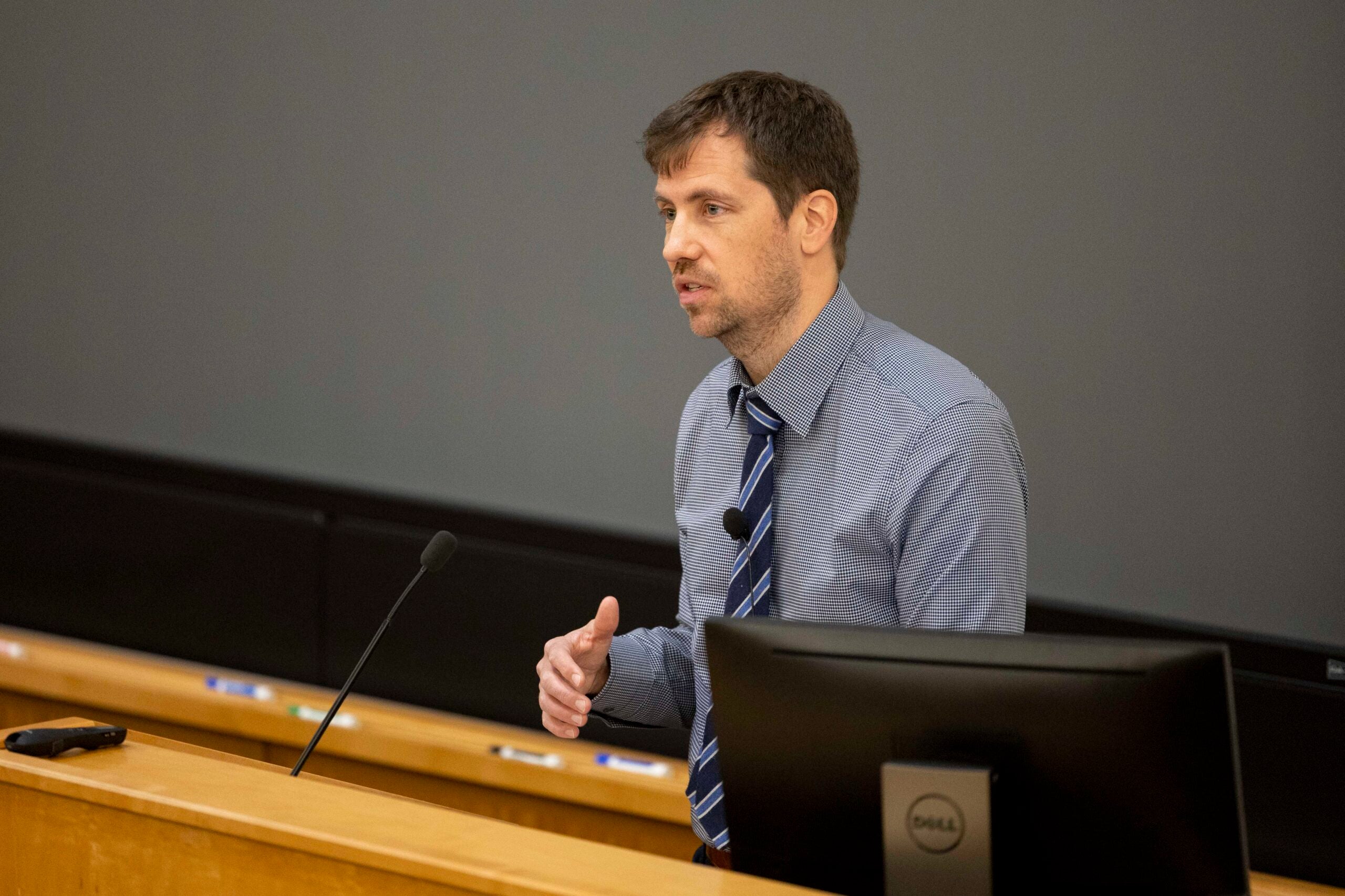
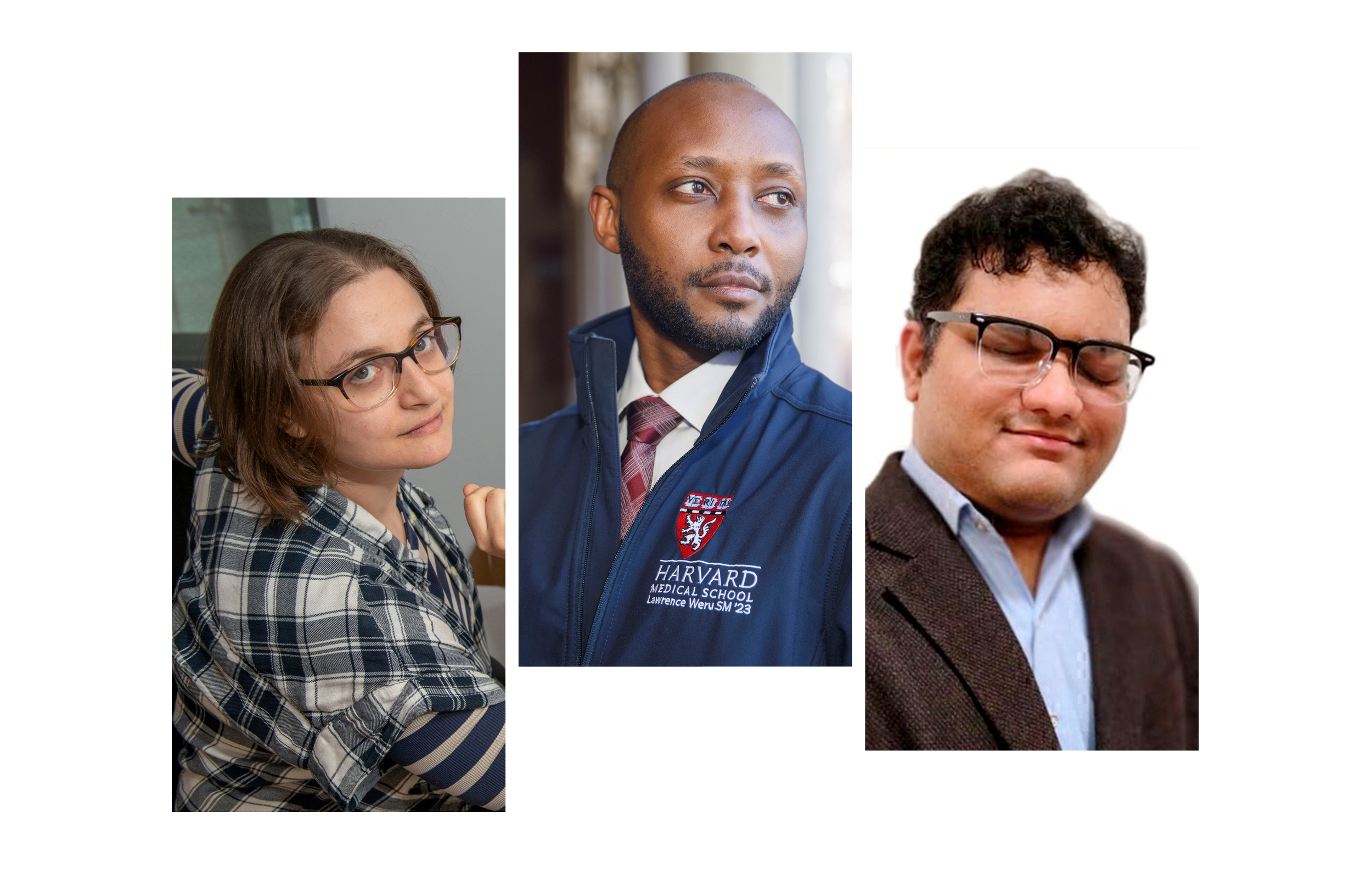
Is AI friend or foe? Wrong question.
A lawyer, a computer scientist, and a statistician debate ethics of artificial intelligence
-
Getting ahead of dyslexia
Harvard lab’s research suggests at-risk kids can be identified before they ever struggle in school
-
Why AI fairness conversations must include disabled people
Tech offers promise to help yet too often perpetuates ableism, say researchers. It doesn’t have to be this way.
-
How did you get that frog to float?
Ever-creative, Nobel laureate in physics Andre Geim extols fun, fanciful side of very serious science
-
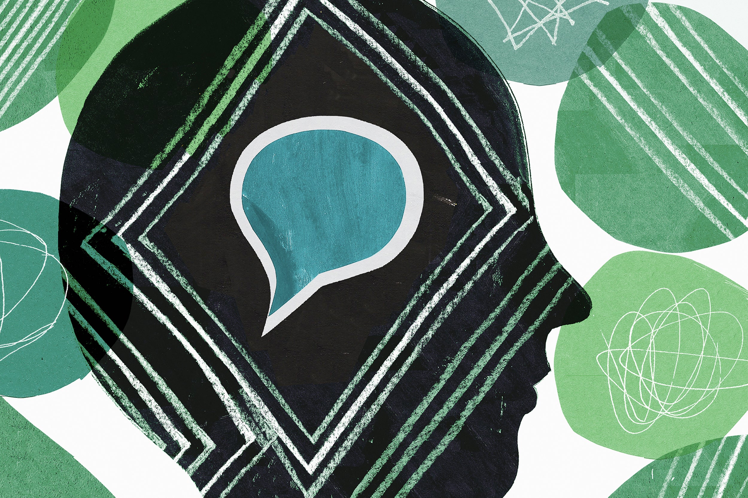
Lifting a few with my chatbot
Sociologist Sherry Turkle warns against growing trend of turning to AI for companionship, counsel
-
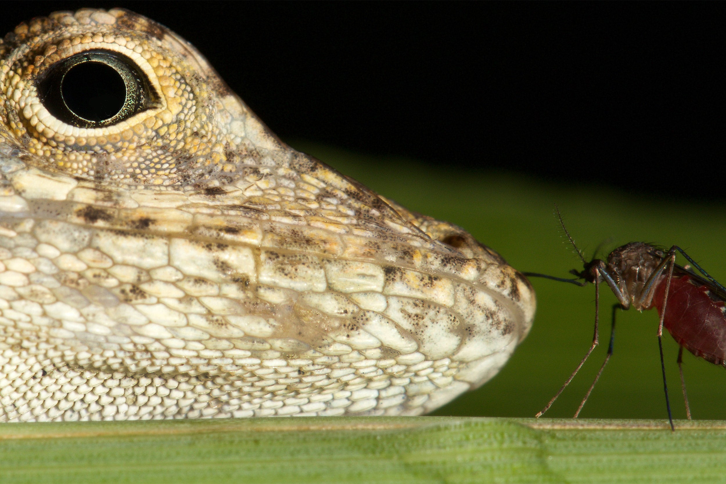
Hate mosquitoes? Who doesn’t? But maybe we shouldn’t.
Entomologist says there is much scientists don’t know about habitats, habits, impacts on their environments
-
Climate alignment is no easy task
Experts at the Salata Institute outline tensions between global and local priorities
-
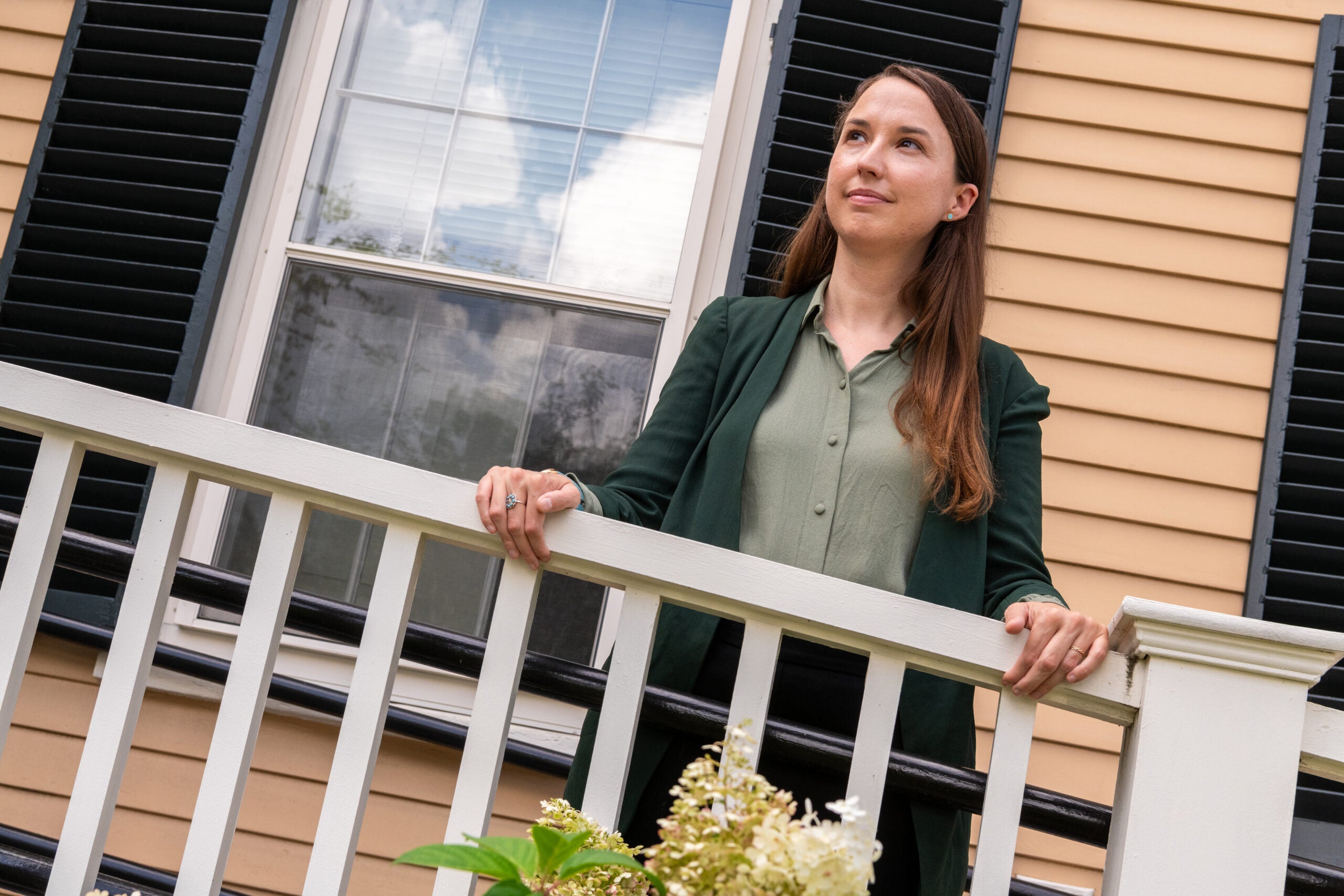
A playbook for policy change
Leah Stokes turns a love for the wilderness into a commitment to help mitigate climate change
-
Under pressure
New tool for precise measurement of superconductors
-
Glimpse into how mind may affect healing
Study finds bruising fades faster in patients who are led to believe more time has passed than actually has

-
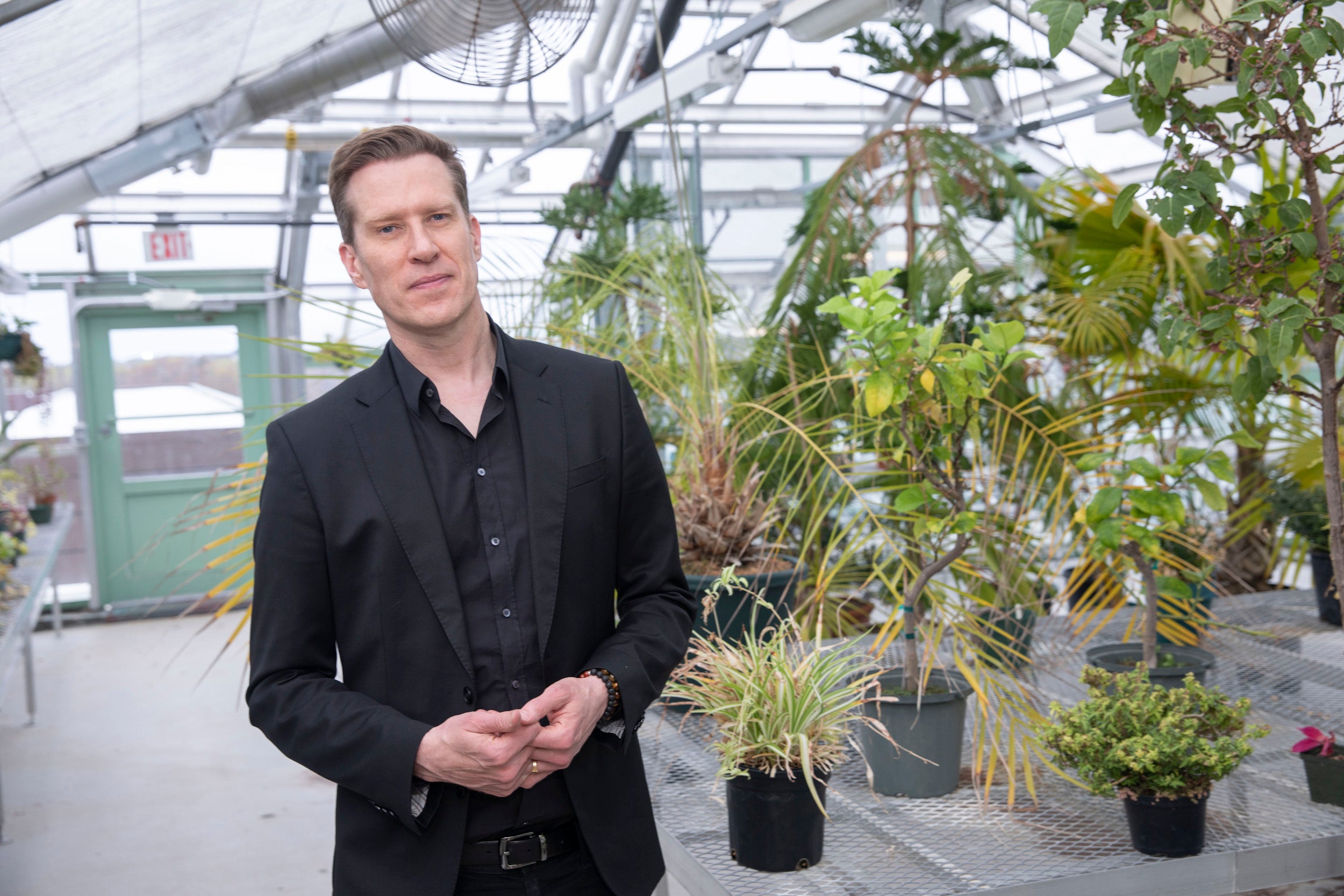
Herbaria’s use and importance grows with climate change
In race against extinction, new agreement supports Harvard’s work to analyze and digitize its medicinal plant collections
-
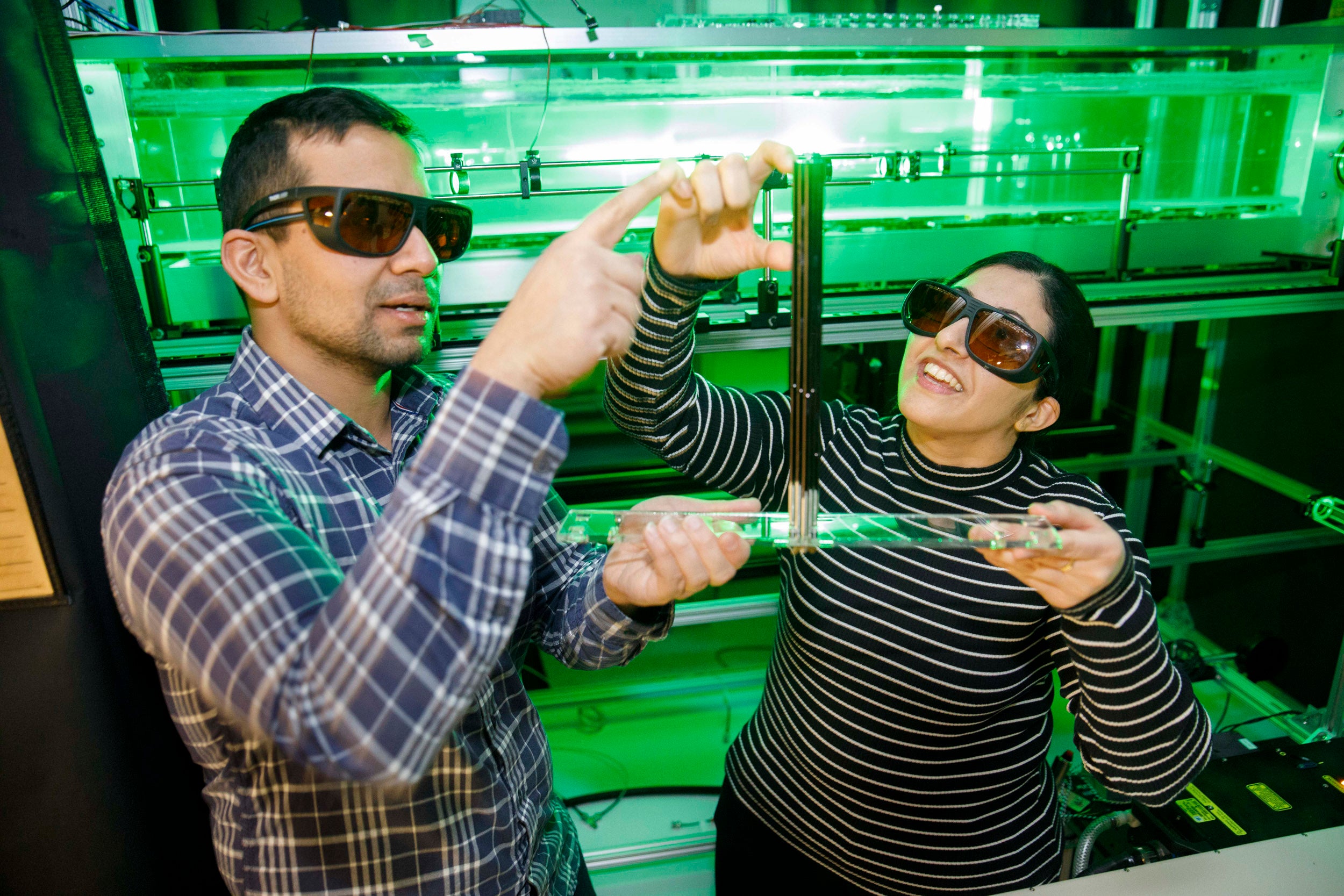
Harvard physicists create a new phase of matter
First demonstration of non-Abelian anyons in a quantum processor
-
Did fermented foods fuel brain growth?
Study puts fermentation, not fire, as pivot point behind our ancestors’ increasing cranial capacity

-
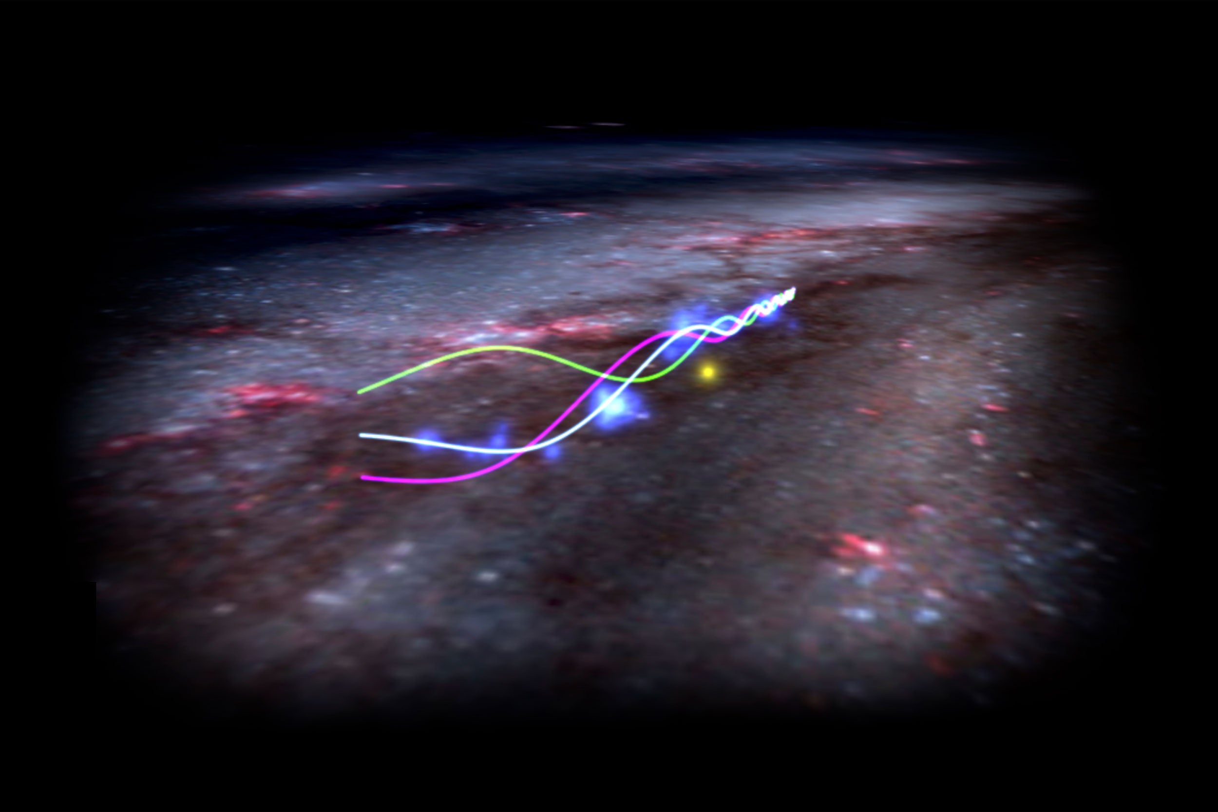
‘Radcliffe Wave’ is waving
Astronomers detail oscillation of our giant neighbor
-
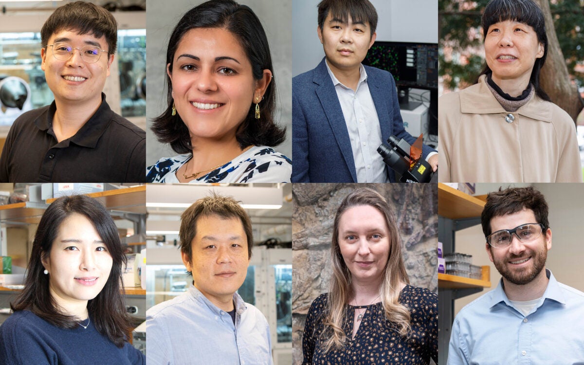
Aramont Fellows bring cutting-edge scientific innovation to the forefront
Four groundbreaking projects investigate brain development, capture raw data with AI, innovate quantum computers, and develop new models to map supernovas
-
Deep in the Amazon, SEAS team tracks a mobile element
Field work on the Rio Negro could help communities exposed to methylmercury protect their food web

-
The miracle of ‘dog’
New findings illuminate complex neuroscience behind even the simplest words, with implications for treatment of speech, language disorders
-
A fast pivot into the unknown
AI’s rapid rise prompts Harvard/MIT Symposium exploring excitement, potential challenges to STEM education, research
-
An evolutionary clue, curled up and long unstudied, in a Harvard museum
Trilobites’ soft undersides show mechanics of early ‘enrollment’ defense
-
Bird’s-eye view of energy conservation
Physics of V-shaped flight formations offer insights into how to improve efficiency of groups of drones, underwater vehicles
-
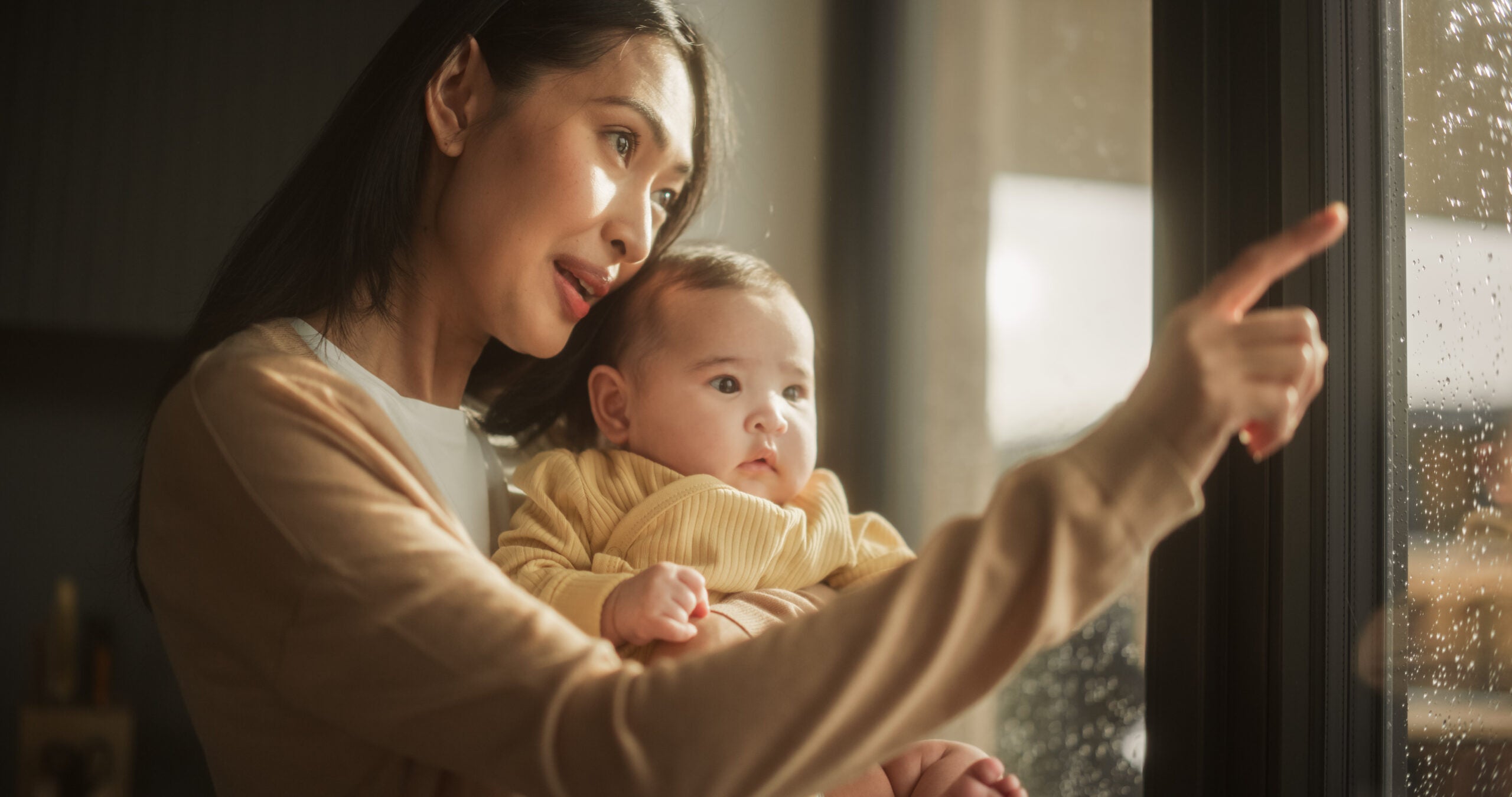
Why do some kids learn to talk earlier than others?
Global study by new faculty Elika Bergelson finds three key predictors of language development. They may surprise you.
-
You did it of your own free will? No such thing.
Neuroscientist Robert Sapolsky says every decision, action you make is result of chain of genes, biology, experience that preceded it
-
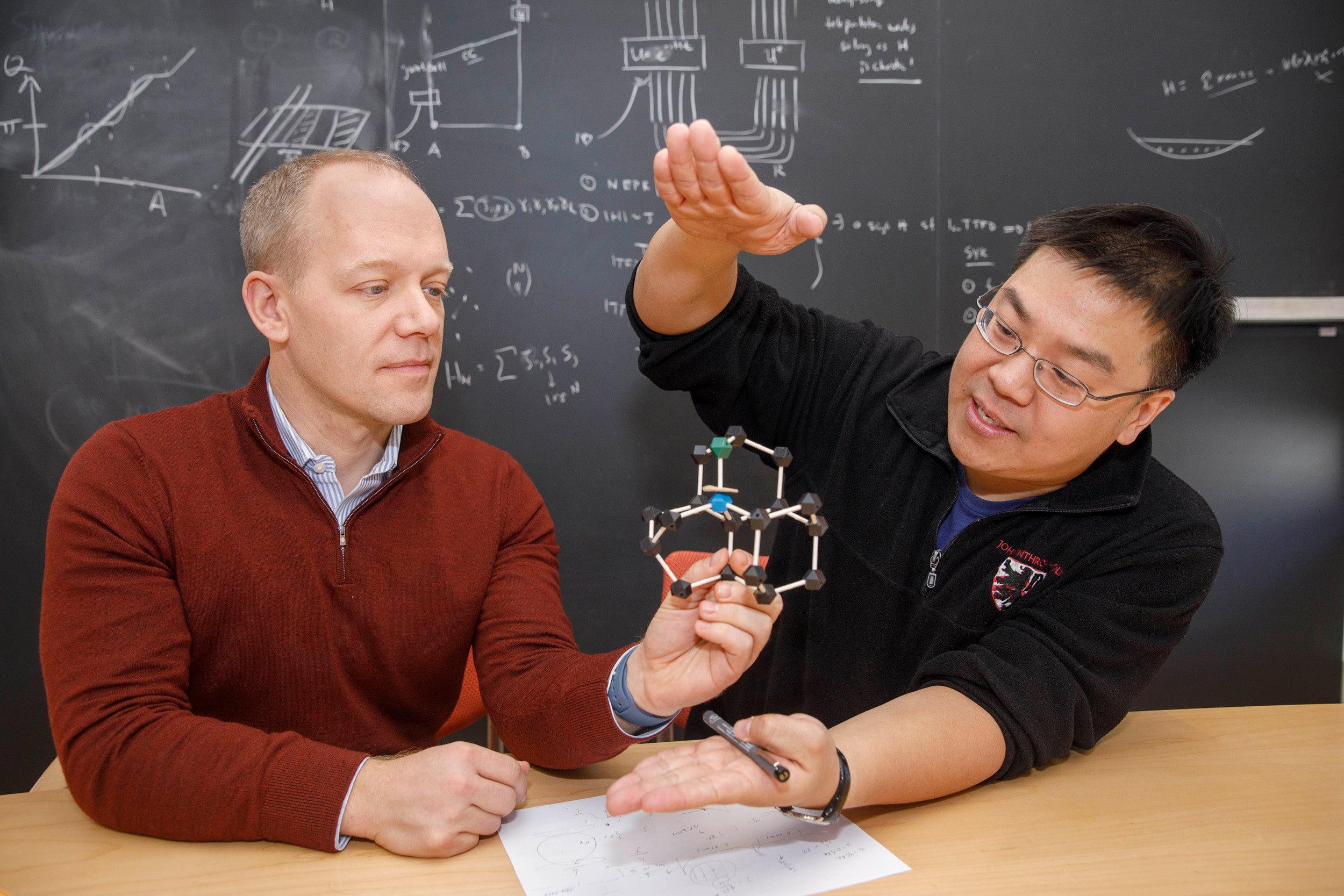
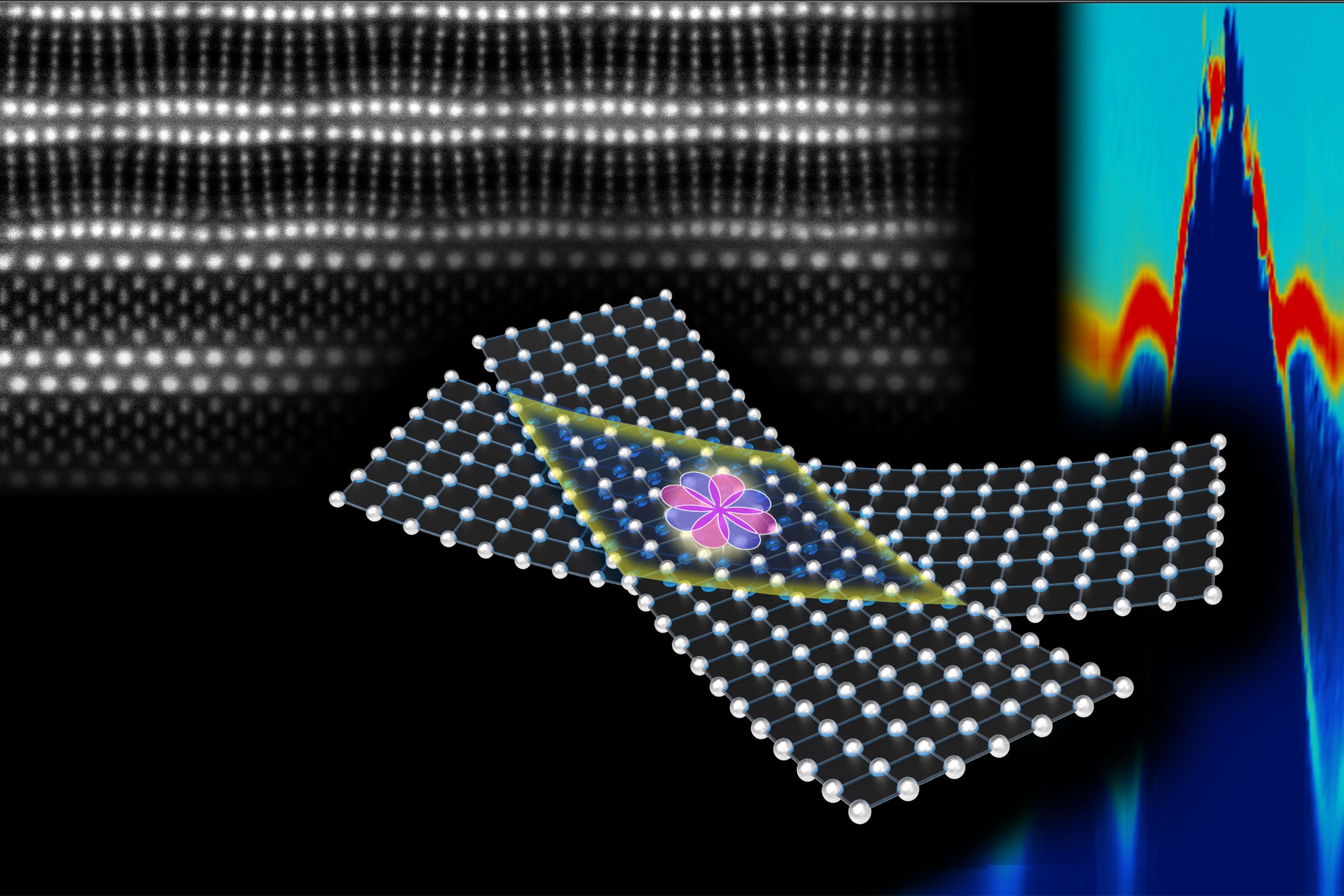
High-temperature superconductors with a twist
Fabrication method could facilitate materials discovery
-
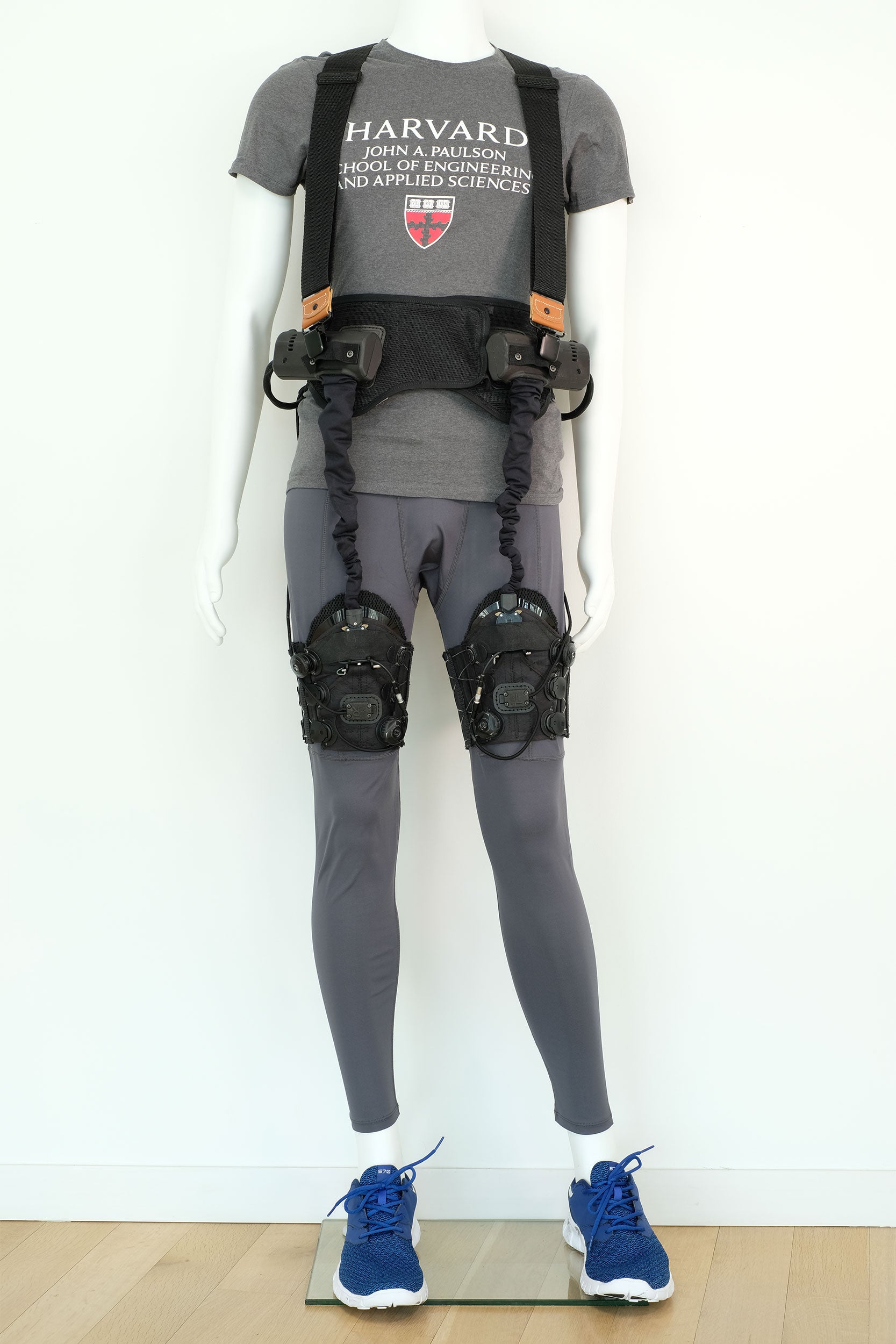
Robotic exosuit gives Parkinson’s patient smoother stride
Eliminates gait freezing, a common and highly debilitating symptom
-
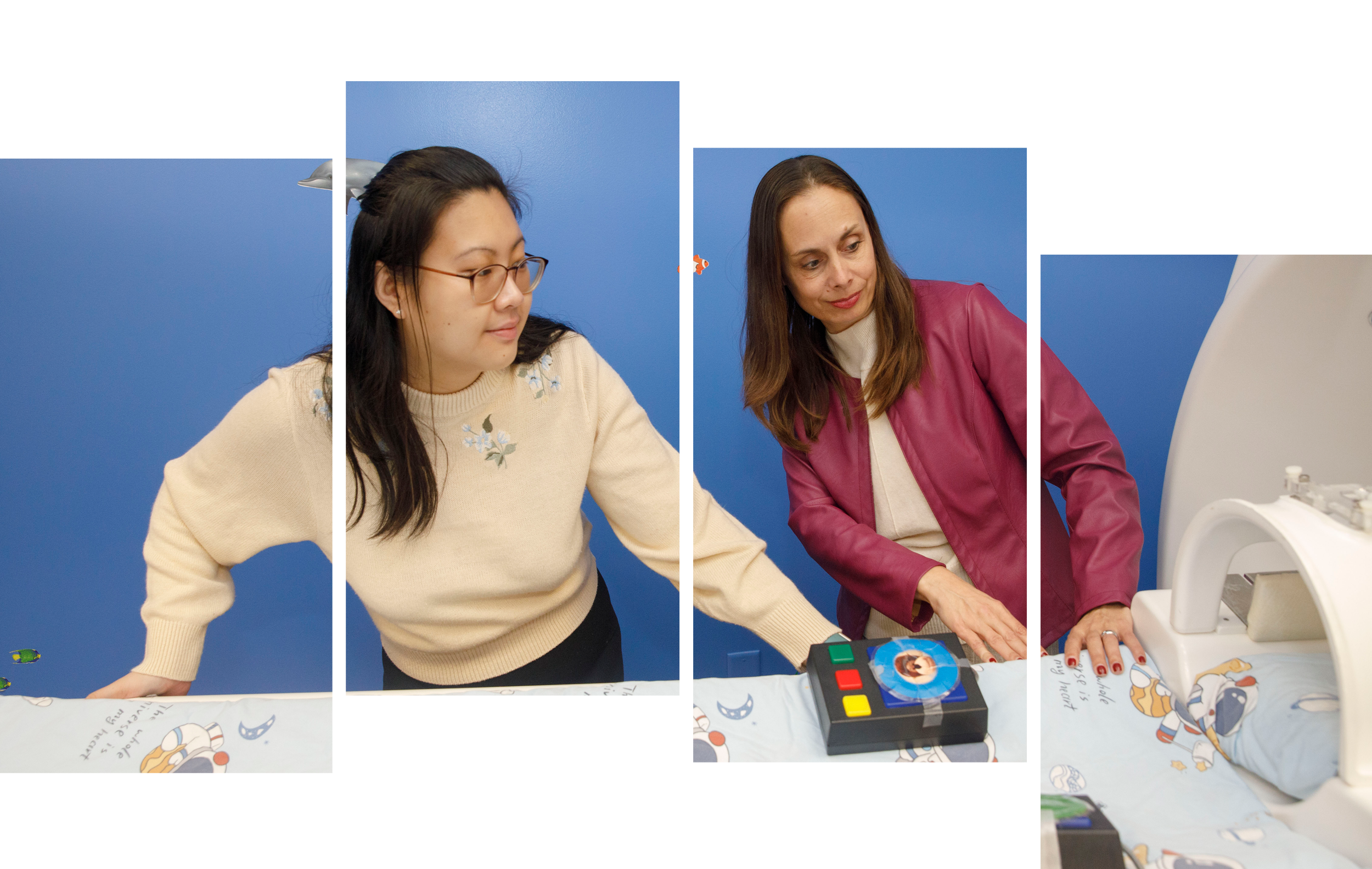
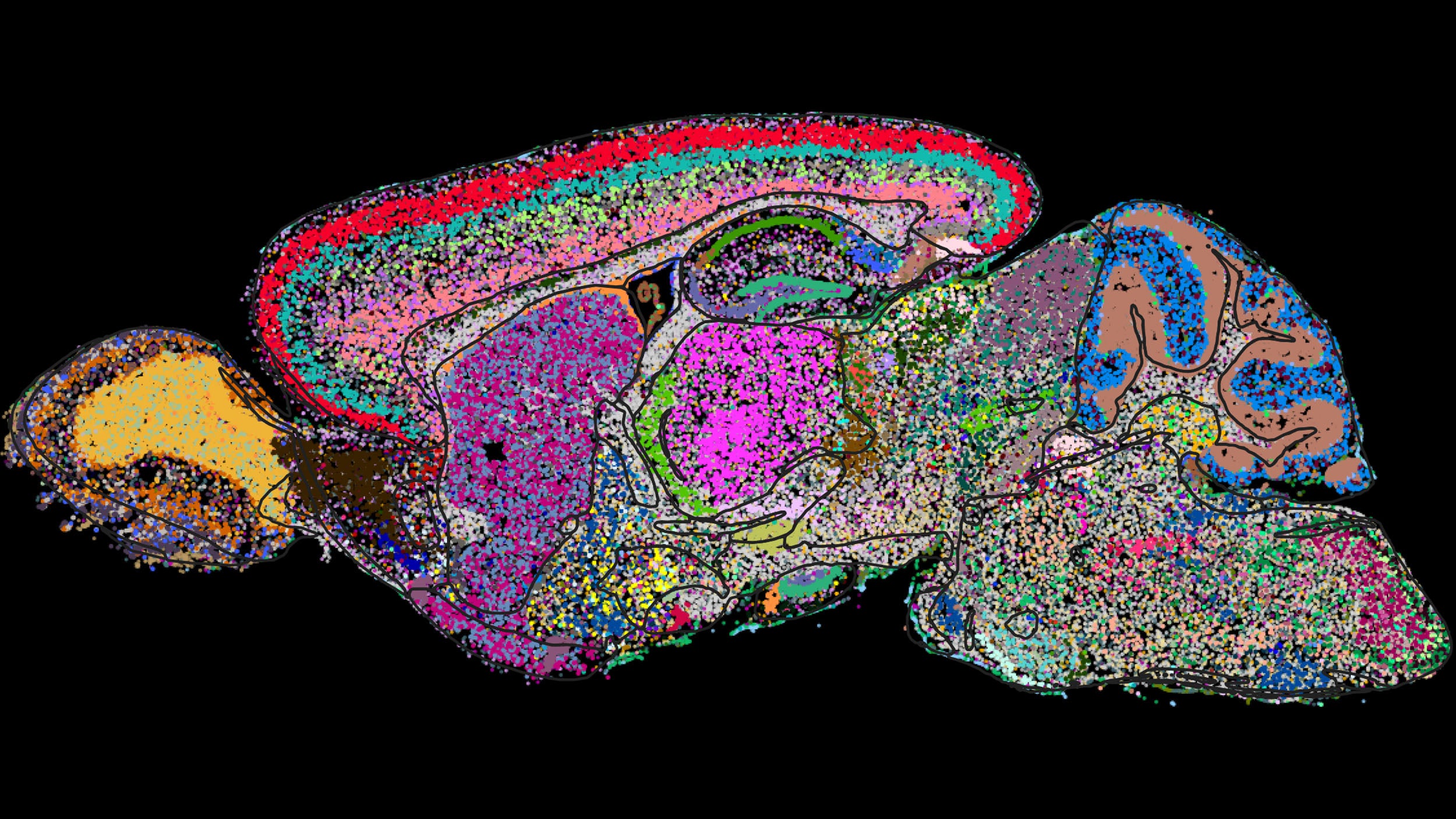
Demystifying a mammal’s brain, cell by cell
Harvard-led team helps create first molecular map for national neuroscience study
-
Researchers create first logical quantum processor
Key step toward reliable, game-changing quantum computing